How Does Via-In-Pad Technology Impact HDI Printed Circuit Board Design?
Technology Impact HDI Printed Circuit Board Design
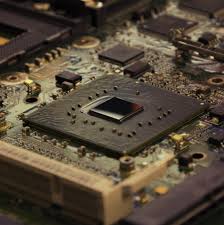
With the increasing use of finer pitch devices and the need for high-density PCBs, via in pad technology is becoming an important aspect of a successful hdi printed circuit board design. It provides a means to reduce component fan out, simplify routing and improve thermal performance. However, using via in pad does add additional complexity and cost to the manufacturing process. As such, it’s essential for designers to fully understand this technology before deciding whether or not it’s the right choice for their project.
In multilayered PCBs, vias are plated holes that connect copper tracks between different layers of the board. There are three main types of vias: through hole vias, blind vias and buried vias. Each type has unique attributes that contribute to the overall optimal performance of a PCB or electronic product. Thru-hole vias connect from the top layer to the bottom, while blind vias are invisible on both surfaces and buried vias are hidden from view under the surface.
The benefits of via in pad are numerous, but the most significant benefit is space conservation. Placing the via directly beneath the pad conserves valuable space that would otherwise be needed for routing signal traces away from the pads. In addition, it eliminates the need for dog-bone routing and significantly lowers the PCB footprint.
How Does Via-In-Pad Technology Impact HDI Printed Circuit Board Design?
Another benefit is improved signal quality. Smaller vias have a lower impedance value, which reduces crosstalk between traces sharing the same via interconnect. This helps to minimize interference between signals and maintain the integrity of the PCB’s design.
Lastly, via in pad can reduce inductance, especially when used for high speed designs. This is because they prevent solder from being pulled into the via and causing unwanted resonances. This technology is particularly useful when used with BGAs because of their small pin size and spacing.
To implement this technology, the PCB must be fabricated with specialized equipment that can drill very small-diameter vias within solder pads. This requires a precise, controlled drilling technique and appropriate plating methods to ensure consistent via depths that provide reliable conductive paths. The vias must also be properly sealed and capped to avoid solder paste contamination during the SMT process.
For this reason, using via in pad is an expensive technology for a normal printed circuit board. However, it can be a good option for high-speed and high-reliability designs that require the smallest possible footprint. Additionally, it’s a great solution for applications where there is limited space for conventional vias, such as micro-BGAs with 0.4mm pitch or smaller. Unlike a through-hole, which requires space between pads for soldering, a via in pad does not. This means that there is no solder wick between the pad and the adjacent pin, so it’s an excellent solution for BGA packages with a very low fanout. In addition, it’s also a great option for high density applications because it allows more connections in a smaller area.